Content:
Multilayer PCB is essential for the advancement of electronic devices, providing a compact yet efficient solution for circuit integration. This arti Multilayer PCB cle will delve into the manufacturing process, features, advantages, usage methods, tips for selecting this product, and ultimately lead to a conclusion.
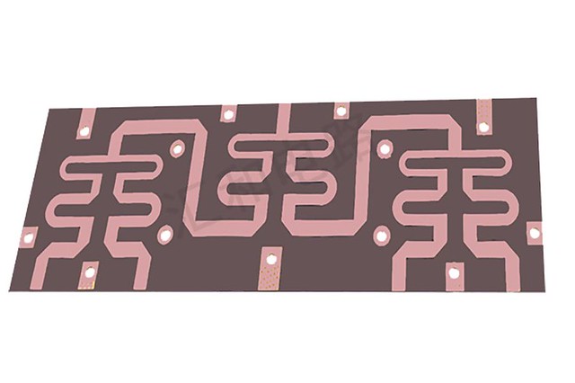
Manufacturing Process:
To create Multilayer PCBs, several layers of copper conductive traces are sandwiched between ins High-density interconnect (HDI) board ulating layers. Unlike Layered PCBs or Double-sided PCBs that only have one or two internal conductive layers respectively, Multilayer PCB boasts multiple internal conductive layers interconnected through vias. These vias enable high-density interconnect (HDI) board production.
Features:
The layered structure of Multilayer PCB not only improves its electrical performance but also enhances its over Layered PCB all durability. Additionally, due to the use of HDI technology in fabrication processes like microvia drilling and laser drilling techniques, smaller via-hole sizes are achievab Multilayer PCB le in comparison to traditional Printed Circuit Boards (PCBs).
Advantages:
1. Increased functionality: With numerous signal paths available within a compact space, Multilayer PCB allows for more complex circuit designs.
2. Enhanced reliability: Improved signal integrity and reduced electromagnetic interference ( Smart door lock supplier EMI) make these boards highly reliable.
3. Size reduction: Compared to other types of rigid boards with equivalent functionality requirements, multilayers can achieve more with less space.
4.Cost-effective manufacturing: Although initially pricier than single-layer or double-layer alternatives when considering material costs alone,Multilayer PCBS benefit from economies-of-scale during assembly stages which offset initial investment costs over time.
Usage Methods:
Multilayer pcb find their application across various industries including telecom Multilayer PCB munications,data storage systems,aerospace &defense systems; medical equipment;servers;audiovisual recording devices,and much more.Their capacity supports high speeds at lower noise levels,making them ideal candidates for advanced digital applications with high-frequency performance demands.
How to Select:
Selecting Smart door lock supplier the proper Multilayer PCB for your application depends on several factors including:
1. Performance requirements: Consider the specific features your product demands in te

rms of impedance control,signal integrity,stability,and heat dissipation capability.
2.Layer count and thickness: Determine the necessary layer count,the overall thickness,and weight requirements based on your project’s complexity.
3.Flexibility versus rigidity: Decide whether you require a flexible des Multilayer PCB ign or a standard rigid board that best suits your space constraints.
Conclusion:
Multilayer PCB plays an integral role in modern electronics by providing compactness, enhanced functionality, and superior reliability. Understanding the manufacturing process, key features, advantages, usage methods, and selection criteria will empower you to make informed decisions when utilizing this technology.Suppliers focused on delivering smart door loc Double-sided PCB k solutions should prioritize sourcing reliable Multilayer PCBA suppliers to ensure optimal performance within their products