
Multilayer Printed Circuit Board
Multilayer printed circuit boards are a popular choice for a wide variety of electronics. They’re especially useful for devices that have many circuits and require a high number of connections.
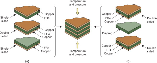
They can be manufactured using a specialized hydraulic press with heated platens. After pressure and heat are applied, a laminate is formed with prepregs and copper foil sheets.
Cost
Compared to single-sided PCBs, multilayer printed circuit boards are more expensive because they require a more complicated manufacturing process. Additionally, they are more difficult to repair if any errors are made during the manufacturing process. This may result in additional labor costs or the need to buy scrap material.
* Industrial: In industrial applications, multilayer PCBs are often used in machinery such as process control and programmable logic controllers. Their durability allows them to withstand harsh environmental conditions such as temperature and pressure. They are also small and lightweight, making them ideal for applications that require high functionality but are designed to be easily transportable.
Consumer: In addition to being durable, multilayer PCBs are popular in several consumer electronics products due to their small size and impressive functionality. This includes smartphones, GPS devices, and other electronics that have to be small and lightweight to function efficiently.
Medical: The medical industry is also heavily reliant on electronic technology, so many of the medical products that come off the production line use multilayer PCBs. These include X-ray equipment, heart monitors, and other medical testing devices.
The medical industry is reliant on portable electronic devices, so multilayer PCBs are particularly helpful in this area as they can be easily transported and are more durable than single-layer options.
In general, a multi-layer PCB is ideal for products that need to be small and lightweight, but they can be used in more complex projects as well. This is because the layers of a multi-layer board allow you to pack more connections into one small space, as opposed to multiple individual boards.
Another important factor in choosing a multi-layer PCB is whether the size and weight of your product matter. If it does, then a multi-layer design is likely the better choice, but if your device will be too large or heavy to function properly with a multi-layer design, then a single-layer PCB may be a better option.
Ultimately, it is up to you and your electronic engineering team to determine which option is best for your project. But, it is always worth examining the cost of multi-layer boards to see if they are the right fit for your needs.
Performance
PCBs have played a major role in the electronics industry since their introduction. Over the years, however, these devices have become increasingly complex in their functions and applications. This has required more specialized PCBs to accomplish these tasks. These specialized PCBs are called multilayer printed circuit boards, and they have a variety of benefits over single and double-sided PCBs.
One of the most important benefits of using a multilayer PCB is that they can be smaller than conventional single or double-sided boards. This makes them ideal for applications in which size is a significant concern.
This is especially true in the modern world where electronics are being designed to be more compact and able to pack more functionality into a smaller space. A multilayer PCB is able to do this because it has more conductive layers per unit area than other types of circuit boards.
Moreover, this helps to keep the weight down. This is important for some applications, like aerospace and defense, where every ounce counts.
Multilayer PCBs are also more durable than other kinds of circuit boards because they have a stronger structure. This allows them to withstand different types of damage and stress, making them ideal for many industries that require them.
A multilayer PCB is more expensive to manufacture than a traditional single or double-sided PCB, but the costs can be offset by the increased efficiency and performance that it offers. The cost can vary based on the design of the board and the multilayer printed circuit board number of layers, and it is important to choose a company that has experience in manufacturing these products.
Multilayer PCBs are an essential part of a number of industries, and they can help to improve the functionality of your product. They are particularly beneficial in the electrical, medical, and telecommunications fields. They can also be used in the automotive, military, and aerospace sectors. They are also commonly found in computers, smartphones, and other consumer products. They have numerous benefits, including the ability to achieve more complex electrical functions, a lighter weight, and better durability.
Design
Whether you’re looking to design your own multilayer PCB or have one custom made for you, it’s important to know what to look for. The number of layers and configuration are important factors that determine the cost, performance and functionality of the final product.
* Industry Trends: With electronics moving ever toward miniaturization yet multi-functional options, multilayer boards have become increasingly popular in recent years. Many consumer products such as smartwatches and universal remotes use these designs instead of traditional single-layer circuits.
These designs offer several advantages over traditional PCBs. For starters, they increase circuit density by allowing multiple components to be soldered onto a board. This results in less waste and increased performance.
It also helps prevent noise, stray capacitance and crosstalk. These benefits are particularly useful for advanced electronics that require high-speed operations.
A multilayer PCB has several conductive layers that are laminated to the dielectric substrate to create a circuit that functions. Each layer has its own copper traces that are thinner than those on the top and bottom layers because they don’t need to carry as much current.
The conductive layers are connected to each other via small holes, called vias. Vias come in various sizes and can be standard, blind or buried.
This allows signal and power traces to pass through the board without winding them around exterior components or other obstacles. The extra layers in a multilayer PCB also open up additional real estate for wiring, which can be critical for advanced devices that need plenty of room to function effectively.
These types of boards are also more durable than single-layer boards and can withstand more harsh conditions. This makes them an ideal choice for military applications and other industrial environments that need high-performing and durable circuitry.
These boards are also commonly used in medical equipments, such as x-ray machines and heart monitors. They’re especially favored in this market for their small size, robust functionality and impressive ability to maintain their functions even when exposed to extreme temperatures.
Production
Multilayer printed circuit boards are made by laminating several layers of PCBs together, and they provide more functionality than single-layered boards. This type of board can be used in a variety of industries, including military and defense, medical devices, and automotive systems.
They also are able to withstand higher heat and pressure than single-layer boards, which makes them more durable and flexible. They are also more costly to produce than standard boards, but they are becoming increasingly popular in the electronics industry.
The production process for a multilayer board begins with the design of the board using PCB designing software such as Eagle, Proteus Altium, and KiCAD. Then, the inner layer core, prepreg multilayer printed circuit board sheets, and copper foil are laminated with the desired thickness using dry film resists and UV light. The lamination process also involves applying pressure, heat, and vacuum using a heated hydraulic press.
After the lamination is complete, the circuitry is covered with a liquid photo imageable (LPI) solder mask. This process prevents solder bridging between different components during assembly. It also protects the copper surface from oxidation.
In the final step of manufacturing, the surface finish is applied to prevent oxidation of the remaining copper areas. This is important because oxidized copper cannot be soldered.
Moreover, it is necessary to ensure that all the holes are drilled properly and accurately. This is done by programming each hole to the drill machine according to the data submitted by the designer.
This is a highly accurate process that requires experienced engineers to execute. The CAM engineer must be able to produce all the drill files, rout files, and image files needed for each individual board.
Additionally, the CAM engineer must generate all the automatic optical inspection (“AOI”) files and test files needed for each stage of the production process. These files are then accessed by machine operators throughout the production process.
The layout of a multilayer PCB can be difficult to produce because of the multiple layers involved in the process. In addition, the symmetry of the layout must be properly maintained to prevent bowing or twisting in the material during heat and pressure.